Studying the electron transport
properties at the electrode|molecule interface under the influence of external
stimuli like electrochemical potential, magnetic field, light, temperature will
have a variety of applications in several research fields like:
(i) Molecular electronics and spintronics: Molecule
based electronic technologies (like OLEDs) and other futuristic molecular
electronics applications (like flexible and transparent electronic devices,
artificial electronic skins etc), where electrode|molecule interface plays a
crucial role in determining performance of the device.
(ii) Energy research: In solar cells, the
charge or electron transfer at electrode|molecule interface plays a
crucial role in determining efficiency. (iii) Electrocatalysis and
photoelectrocatalysis: Activity/selectivity of a catalyst depends on the
effectiveness of charge transport at electrode|catalyst interface under the
influence of electrochemical potential and/or light.
(iv) Sensors:Sensitivity and selectivity of a
sensor may depend on the effective charge transport at electrode|molecule
interface.
Thus, the ability to measure and control charge
transport across metal|molecule interface is of considerable fundamental
interest. In our group, we
focus on developing the instrumentation and experimental
methodology to study the charge/heat transport properties at the
electrode|molecule interface (at a single molecule or ensemble
level) under the influence of external stimuli.
We are aiming at constructing a detailed knowledge base of the physico-chemical
properties of molecular junctions and the mechanistic insights behind the
single (or ensemble) charge/heat transport. Such knowledge is the key to design
the next generation of hybrid electronic high-performance devices for a wide
variety of applications. Such knowledge is strongly desirable because of the
imminent potential of single (or ensemble) molecular junctions as the prototype
building block for functional materials and molecular electronic devices. The
aim of our research work is to contribute to that knowledge.
By studying the electronic properties at various level
of complexity from single molecule to single cell, Structure property
relationships can be established. Using these established structure property
relations, we will finally explore the ways in which these relations can be
translated to the real-world applications and will help to solve the unwound
mysteries of the nature. We are trying to reveal how atomic-detailed nano-scaled
structural modification in materials can affect the performance, energy consumption
and longevity of molecular-scale devices. In terms of the practical point of
view, our research holds a great the promise of developing flexible,
lightweight, solution-processable, and low-cost molecular devices.
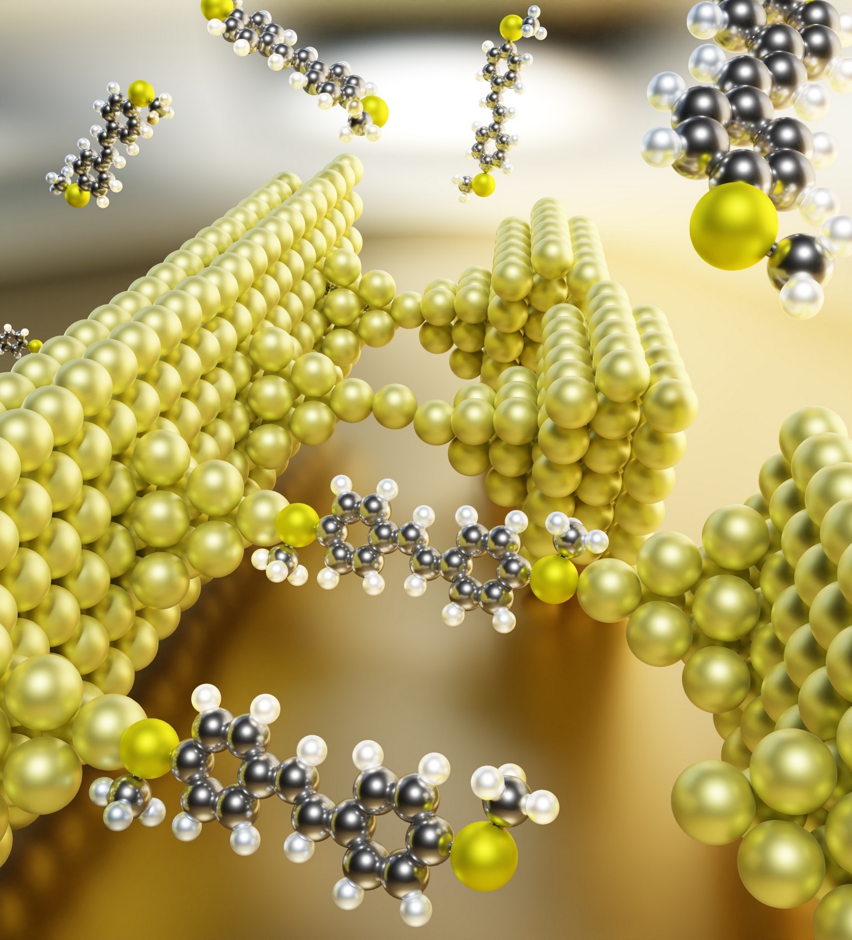
Measuring the charge transport/heat transport through a single molecule at room
temperature under ambient conditions poses various experimental challenges.
This needs a sophisticated instrumentation capable of trapping the molecule
between two electrodes and simultaneously measuring the current/heat passing
through this junction with very high accuracy and precision. Since the
molecule trapped between two electrodes at ambient conditions are subjected to
thermal vibrations, as the result the lifetime of the metal|molecule| metal
junction is of the order of 10-100s of milli-seconds. Any external mechanical
instability will further decrease the stability of the metal|molecule|metal
junction at the nanoscale makes it impossible to successfully measure the electronic/heat
transport through the junctions. Thus, in order to probe the electronic/heat
transport through the single molecular junction, a highly stable, robust and
high frequency/sampling measurement system is required. We have designed and
built a Mechanically controlled break junction (MCBJ) and scanning tunneling
microscope break junction setups (STM-BJ) which provide this experimental
capability.
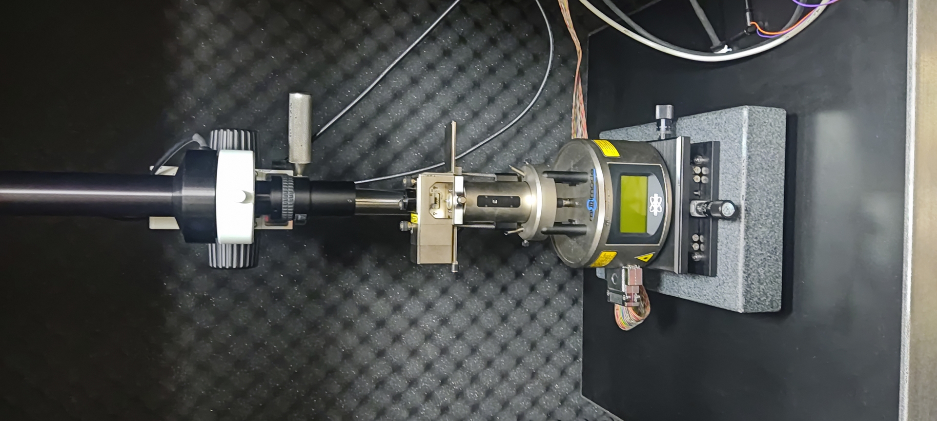
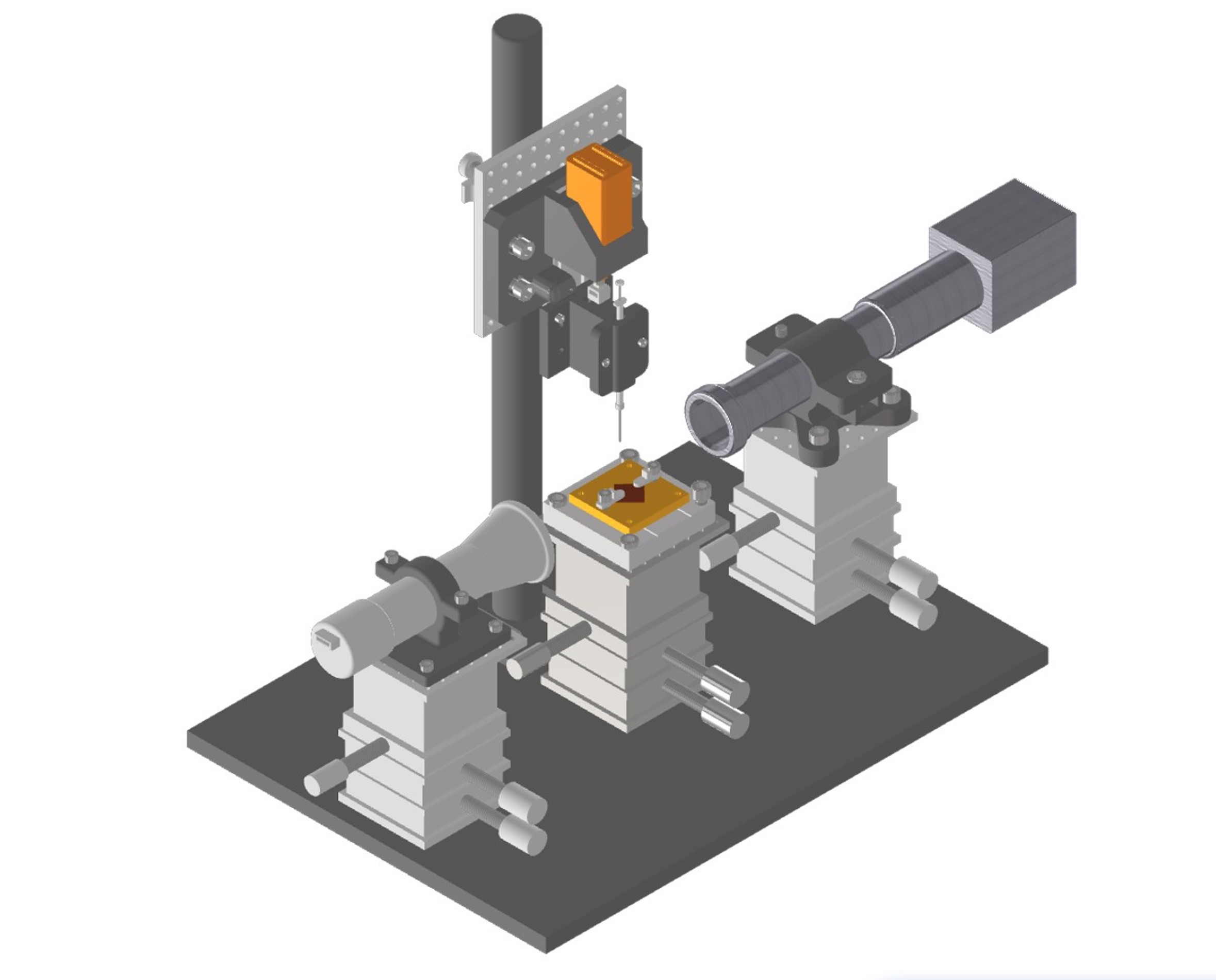
1.Mechanically controlled
break junction setup: In mechanically controlled break junction experiment,
a nanosized gap is created between two gold electrodes by pushing the spring
steel substrate from below on which gold wire notched in the middle is mounted
(fixed) at two positions by epoxy resin. The nano resolution pushing of the
spring steel is done with the help of suitable piezo stack which expands upon
applying positive potential and contracts upon applying negative potential. The
coarse movement is done with the help of Stepper motor on the axel of with
piezo stack is attached for fine movement. Upon pushing the spring steel from
below the attached gold wire (0.1 mm) breaks and an adjustable nanosized gap is
created. When the nano gap is in comparison of the target molecule length, the
anchoring groups of molecules (like thiol, pyridine etc.) attaches to gold
electrodes. Upon more pushing the steel substrate the gap is enlarged as a
result of which the molecule detaches from the electrode(s) and the junction is
broken. Using current as feedback the instrument senses the broken junction and
starts contracting the piezo. As a result, the gap reduces again, and the
molecule is again trapped. Upon further decreasing the nanogap between two
electrodes eventually, the 2 electrodes touch each other, and a short circuit
current is measured. Then the opening cycle is repeated. These opening and
closing cycles are repeated thousands of times to get statistically significant
data. The speed of opening and closing the gap and the frequency of data
collection of current upon applying potential across the gold electrodes is
controlled by careful movement of piezo stack and frequency adjustment in data
collection system. Modular design of our setup allows us to couple our MCBJ
with other instruments like Raman microscope to probe the spectroscopic
signatures of molecular junctions and also we can incorporate external light
source or magnetic field or temperature to stimulate/tune the charge transport
properties.
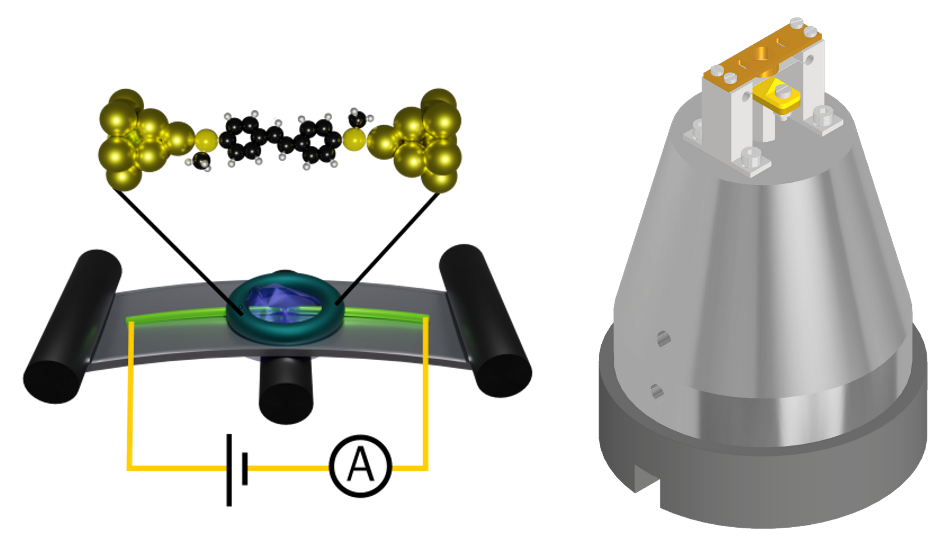
2.Scanning tunneling microscope break junction setup: In this setup a nanogap is created between a bottom flat electrode and top thin wire electrode (with single atom thick tip). The movement of the top electrode is controlled by the piezo stack and stepper motor combination. Using this setup we can perform the single molecular conductance measurements under electrochemical conditions. Additionally, this setup also allows the heating of bottom electrode to create a temperature gradient across the molecular junction to measure the thermopower generated by single molecules attached to two electrodes at different temperatures.
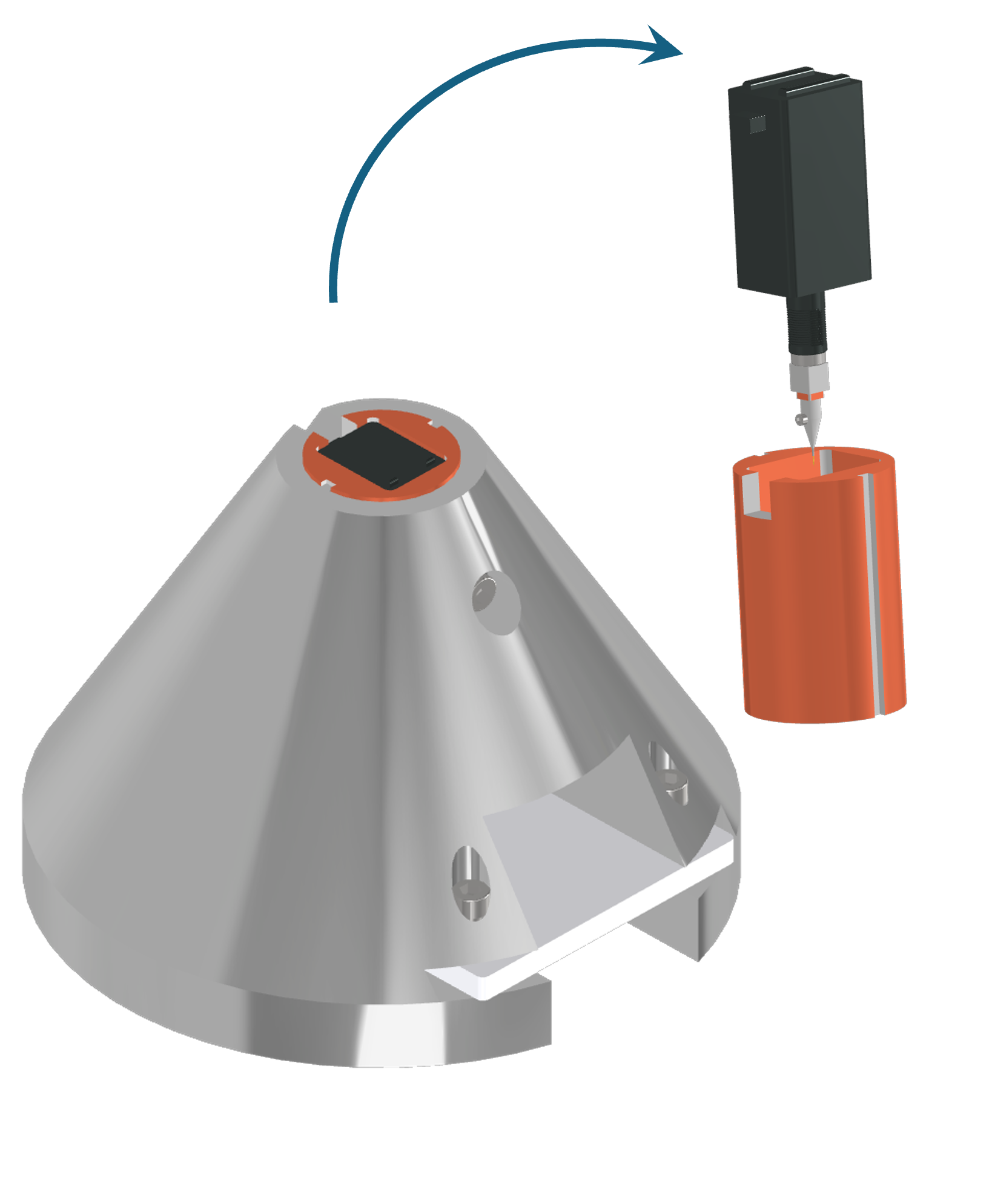
3.EGaIn based thermo-electric set-up: This setup is capable of simultaneous measurement of electric conductance and Thermoelectric power measurement of SAM based junctions. The top Electrode is based on non-Newtonian liquid metal, an Eutatic mixture(75.5% Ga and 24.5% In by weight) of Gallium and Indium(EGaIn), covered with a conductive, self-passivating Ga2O3 layer (nominal thickness of ∼1 nm). The EGaIn conical tip enables reproducible, noninvasive, and well defined top contacts on delicate molecular thin films such as self-assembled monolayers (SAMs) under ambient conditions. The top electrode is obtained as a hanging EGaIn conical tip from a micro-syringe containing bulk mixture. Template stripped Au/Ag(111) Surface act as bottom electrode, on which self-assembled monolayer is deposited. Using this setup we explore the transport through ensemble molecular junctions and these experiments are complementary to our single molecular work.
4. Atomic force microscopy: We also have a Bruker multi-mode STM/AFM setup. We use this setup to study morphology and electromechanical properties of molecular thin films. We are also developing electrochemical conducting probe AFM, to study the electromechanical properties of nanoscale systems with relevance to energy research.